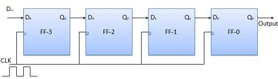
A memory is just like a human brain. It is used to store data and instruction. Computer memory is the storage space in computer where data is to be processed and instructions required for processing are stored.
The memory is divided into large number of small parts. Each part is called a cell. Each location or cell has a unique address which varies from zero to memory size minus one.
For example if computer has 64k words, then this memory unit has 64 * 1024 = 65536 memory location. The address of these locations varies from 0 to 65535.
Memory is primarily of two types
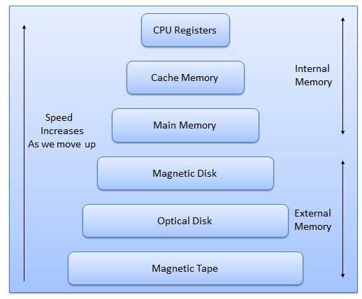
Characteristics of Memory Hierarchy are following when we go from top to bottom.
- Capacity in terms of storage increases.
- Cost per bit of storage decreases.
- Frequency of access of the memory by the CPU decreases.
- Access time by the CPU increases.
RAM
A RAM constitutes the internal memory of the CPU for storing data, program and program result. It is read/write memory. It is called random access memory (RAM).
Since access time in RAM is independent of the address to the word that is, each storage location inside the memory is as easy to reach as other location & takes the same amount of time. We can reach into the memory at random & extremely fast but can also be quite expensive.
RAM is volatile, i.e. data stored in it is lost when we switch off the computer or if there is a power failure. Hence, a backup uninterruptible power system (UPS) is often used with computers. RAM is small, both in terms of its physical size and in the amount of data it can hold.
RAM is of two types
- Static RAM (SRAM)
- Dynamic RAM (DRAM)
Static RAM (SRAM)
The word static indicates that the memory retains its contents as long as power remains applied. However, data is lost when the power gets down due to volatile nature. SRAM chips use a matrix of 6-transistors and no capacitors. Transistors do not require power to prevent leakage, so SRAM need not have to be refreshed on a regular basis.
Because of the extra space in the matrix, SRAM uses more chips than DRAM for the same amount of storage space, thus making the manufacturing costs higher.
Static RAM is used as cache memory needs to be very fast and small.
Dynamic RAM (DRAM)
DRAM, unlike SRAM, must be continually refreshed in order for it to maintain the data. This is done by placing the memory on a refresh circuit that rewrites the data several hundred times per second. DRAM is used for most system memory because it is cheap and small. All DRAMs are made up of memory cells. These cells are composed of one capacitor and one transistor.
ROM
ROM stands for Read Only Memory. The memory from which we can only read but cannot write on it. This type of memory is non-volatile. The information is stored permanently in such memories during manufacture.
A ROM, stores such instruction as are required to start computer when electricity is first turned on, this operation is referred to as bootstrap. ROM chip are not only used in the computer but also in other electronic items like washing machine and microwave oven.
Following are the various types of ROM −
MROM (Masked ROM)
The very first ROMs were hard-wired devices that contained a pre-programmed set of data or instructions. These kind of ROMs are known as masked ROMs. It is inexpensive ROM.
PROM (Programmable Read Only Memory)
PROM is read-only memory that can be modified only once by a user. The user buys a blank PROM and enters the desired contents using a PROM programmer. Inside the PROM chip there are small fuses which are burnt open during programming. It can be programmed only once and is not erasable.
EPROM (Erasable and Programmable Read Only Memory)
The EPROM can be erased by exposing it to ultra-violet light for a duration of upto 40 minutes. Usually, an EPROM eraser achieves this function. During programming an electrical charge is trapped in an insulated gate region. The charge is retained for more than ten years because the charge has no leakage path. For erasing this charge, ultra-violet light is passed through a quartz crystal window (lid). This exposure to ultra-violet light dissipates the charge. During normal use the quartz lid is sealed with a sticker.
EEPROM (Electrically Erasable and Programmable Read Only Memory)
The EEPROM is programmed and erased electrically. It can be erased and reprogrammed about ten thousand times. Both erasing and programming take about 4 to 10 ms (millisecond). In EEPROM, any location can be selectively erased and programmed. EEPROMs can be erased one byte at a time, rather than erasing the entire chip. Hence, the process of re-programming is flexible but slow.
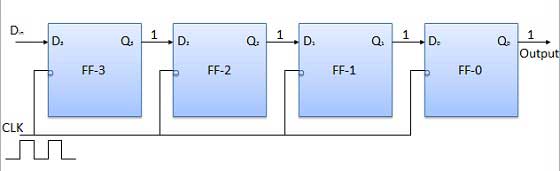
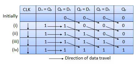
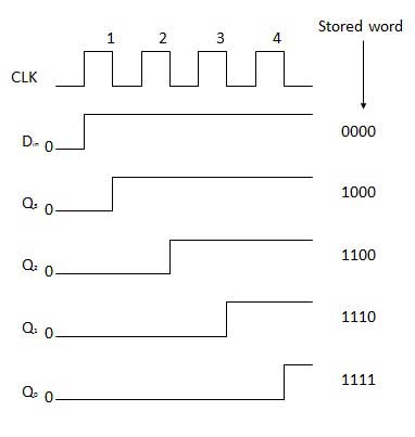
Serial Access Memory
Sequential access means the system must search the storage device from the beginning of the memory address until it finds the required piece of data. Memory device which supports such access is called a Sequential Access Memory or Serial Access Memory. Magnetic tape is an example of serial access memory.
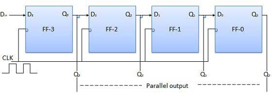
Direct Access Memory
Direct access memory or Random Access Memory, refers to conditions in which a system can go directly to the information that the user wants. Memory device which supports such access is called a Direct Access Memory. Magnetic disks, optical disks are examples of direct access memory.
Cache Memory
Cache memory is a very high speed semiconductor memory which can speed up CPU. It acts as a buffer between the CPU and main memory. It is used to hold those parts of data and program which are most frequently used by CPU. The parts of data and programs, are transferred from disk to cache memory by operating system, from where CPU can access them.
Advantages
- Cache memory is faster than main memory.
- It consumes less access time as compared to main memory.
- It stores the program that can be executed within a short period of time.
- It stores data for temporary use.
Disadvantages
- Cache memory has limited capacity.
- It is very expensive.
Virtual memory is a technique that allows the execution of processes which are not completely available in memory. The main visible advantage of this scheme is that programs can be larger than physical memory. Virtual memory is the separation of user logical memory from physical memory.
This separation allows an extremely large virtual memory to be provided for programmers when only a smaller physical memory is available. Following are the situations, when entire program is not required to be loaded fully in main memory.
User written error handling routines are used only when an error occurred in the data or computation.
Certain options and features of a program may be used rarely.
Many tables are assigned a fixed amount of address space even though only a small amount of the table is actually used.
The ability to execute a program that is only partially in memory would counter many benefits.
Less number of I/O would be needed to load or swap each user program into memory.
A program would no longer be constrained by the amount of physical memory that is available.
Each user program could take less physical memory, more programs could be run the same time, with a corresponding increase in CPU utilization and throughput.
Auxiliary Memory
Auxiliary memory is much larger in size than main memory but is slower. It normally stores system programs, instruction and data files. It is also known as secondary memory. It can also be used as an overflow/virtual memory in case the main memory capacity has been exceeded. Secondary memories cannot be accessed directly by a processor. First the data/information of auxiliary memory is transferred to the main memory and then that information can be accessed by the CPU. Characteristics of Auxiliary Memory are following −
Non-volatile memory − Data is not lost when power is cut off.
Reusable − The data stays in the secondary storage on permanent basis until it is not overwritten or deleted by the user.
Reliable − Data in secondary storage is safe because of high physical stability of secondary storage device.
Convenience − With the help of a computer software, authorised people can locate and access the data quickly.
Capacity − Secondary storage can store large volumes of data in sets of multiple disks.
Cost − It is much lesser expensive to store data on a tape or disk than primary memory.